


For a long time now, I have been interested in devices to be used for personal organisation. Mobile phones contain too much distraction and are an attention drain, one minute you are checking an email, the next hour you just doom scrolled 30 second videos. It’s just insane.
What I want is a device that is limited by design to productivity, is simple and can be built/hacked as features are needed. To be useful as a productivity device, it needs to be able to connect to systems outside of itself easily.
Additionally, I want to re-use the developed circuits elsewhere.
The overall problem that we are trying to solve is the following:
A small productivity watch that is internet connected, to perform a series of lightweight tasks that are synced with other devices via the internet.
Examples of tasks of interest:
Maybe I can think of other things, but I think these are already useful services!
I have used some other devices…
For over a year I was using the Pinetime, based on JF002’s InfiniTime software.
The hardware is pretty good, but lacks WiFi. The only way to have this device communicating with the outside world is to connect to another device via Bluetooth, which limits the usefulness of the device.
The software is interesting, but it is all baked into a large mono-repo. I have nothing against this idea, but there is no real clean idea of what an app is, and what the OS is. Probably one of the biggest sins is that if you accidentally flash a bad firmware, it is possible to brick your device.
Probably the most promising way forwards is wasp-os which is based on micropython, but the hardware still suffers the same issue of connectivity.
I am working with the T-Watch S3 for another project in micropython. The only real complaint with the device is the cost and the watch strap (I have quite sensitive skin).
One possible issue is that the device offers too much, to say that it would be possible to have chats on it and do mobile-phone-esque tasks with it.
Now for the chosen parts…
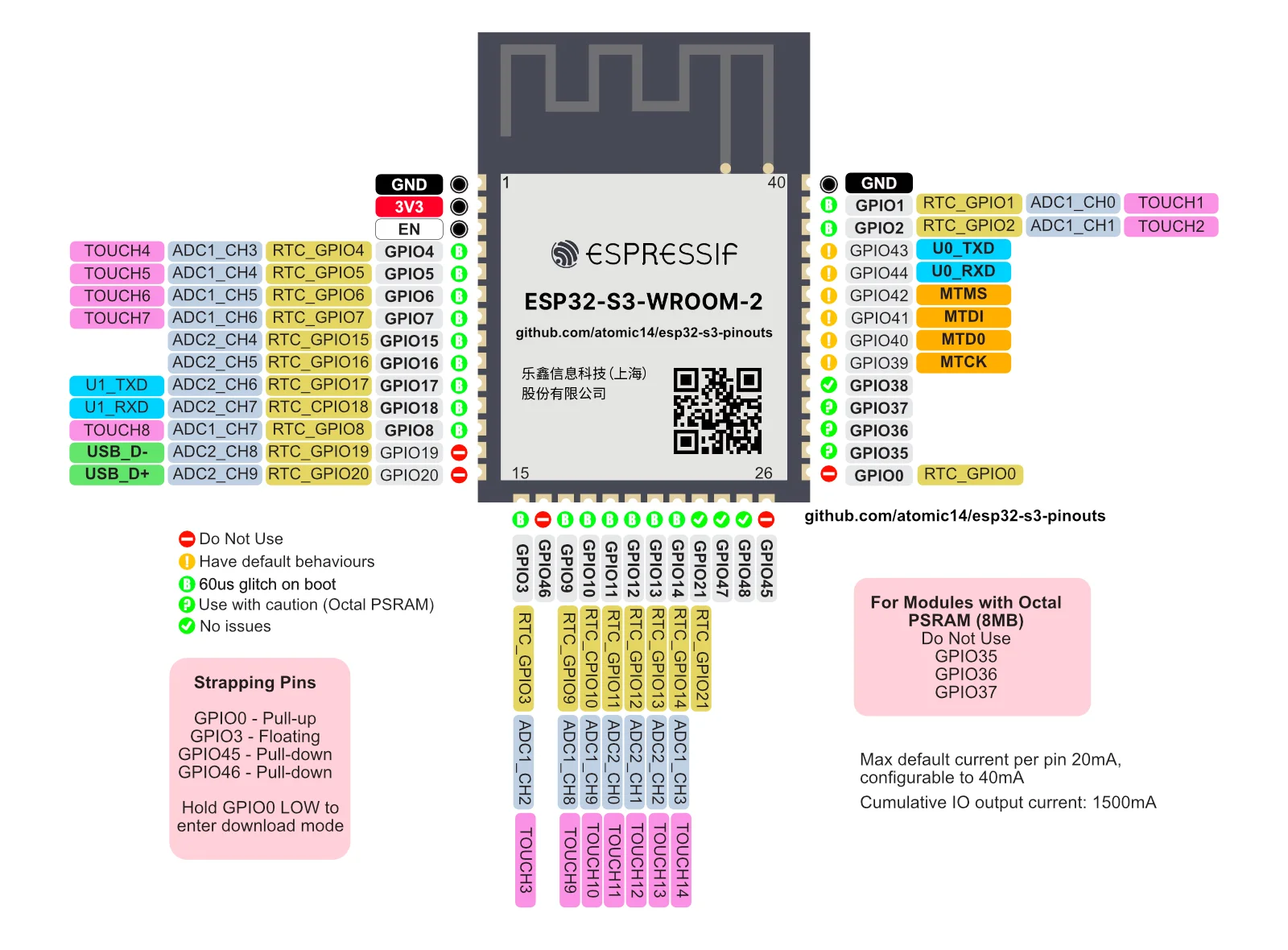
The main controller chosen is the ESP32-S3-WROOM-1. It runs micropython quite well from previous experience.
The battery is 30mAh 401012 (dimensions: 4mm x 10mm x 12mm). Assuming a total on time of 30 seconds per hour at 300mAh, and assuming the system is in a light sleep or lower with ~1mAh draw, we can expect the system to run on a full charge for:
0001 batt_mAh = 30
0002 on_mAh = 260 # WiFi average peaks
0003 off_mAh = 1
0004 on_ratio = 0.5 / 60 # minutes per hour
0005 usage_mAh = (on_ratio * on_mAh) + ((1 - on_ratio) * off_mAh)
0006
0007 hours = batt_mAh / usage_mAh
0008 print("Expected usage of " + str(hours) + " hours")
Expected usage of 9.49868073878628 hours
Then we are just touching on a 10 hour operating time.
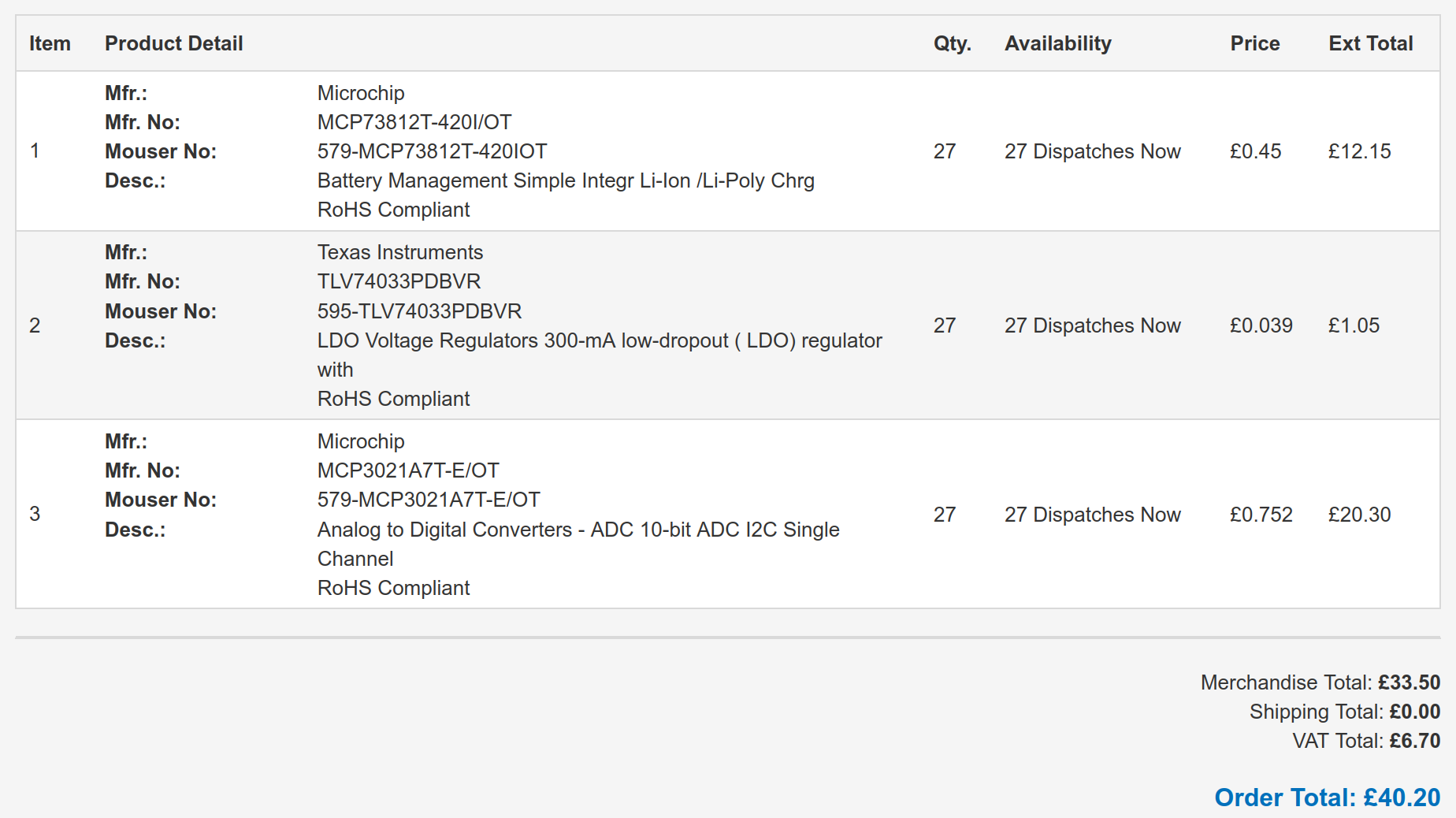
The ADC IC is the MCP3021A7T-E/OT which takes a supply between 2.7V and 5.5V, and can read within the same range. Foreshadowing: It is not not be.
The voltage regulator is the TLV74033PDBVR, chosen because it is just 8 pence. It’ll take an input between 1.4V and 5.5V and produce a 3.3V voltage. It will output 300mA, which exactly matches the expected spike current from the ESP32 during WiFi. There is no absolute maximum current specified, so I assume we can maybe push the envelope slightly.
Otherwise the next highest current eating device is the 0.96” OLED display with the SSD1306 driver, requiring ~20mA of power at maximum contrast. Everything else is sipping power.
The chosen battery charging circuit is the MCP73812T-420I/OT, which should charge a single cell LiPo at 50mA when the USB supply is provided. It has constant voltage, constant current, thermal regulation, etc.
The first thing to notice is that it is a two-layer board and everything is mounted single-side. This means that it can be manufactured simply on a hot plate. The width and depth ~4cm x ~4cm, and the height will likely be defined by the top of the OLED to the bottom of the soldered through-hole headers. Offering the OLED to an existing board shows a height ~17mm. The battery should fit nicely under the display.
As you can see, I have chosen a ESP32 module and not the chip, so it is certified and could be sold. The ESP32 module does take up the majority of the design, though.
The only traces that were manually routed were the USB differential pair, and if you look closely, there is a length matching wiggle near the USB socket. It should be close enough for basic USB 2 communications.
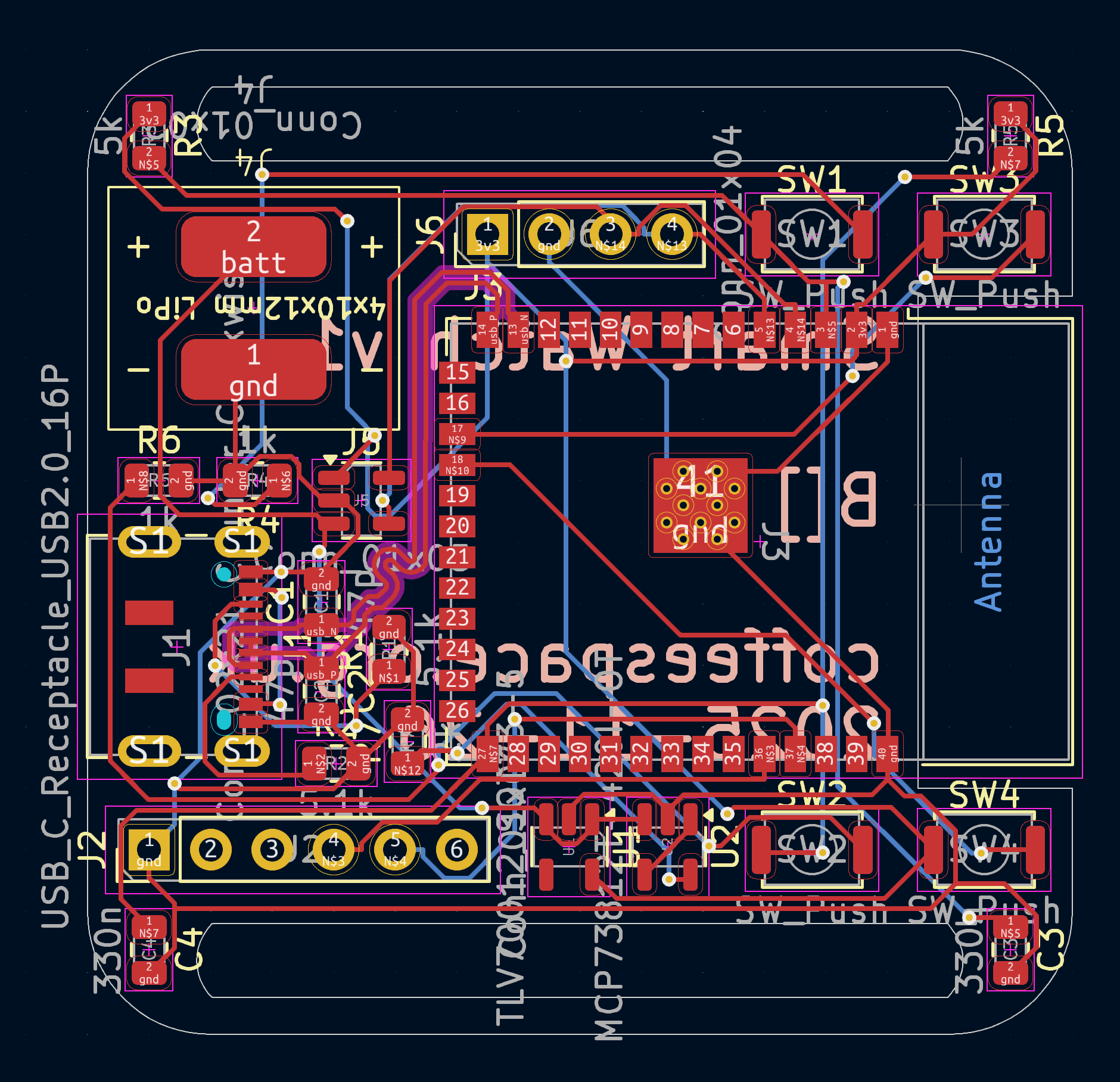
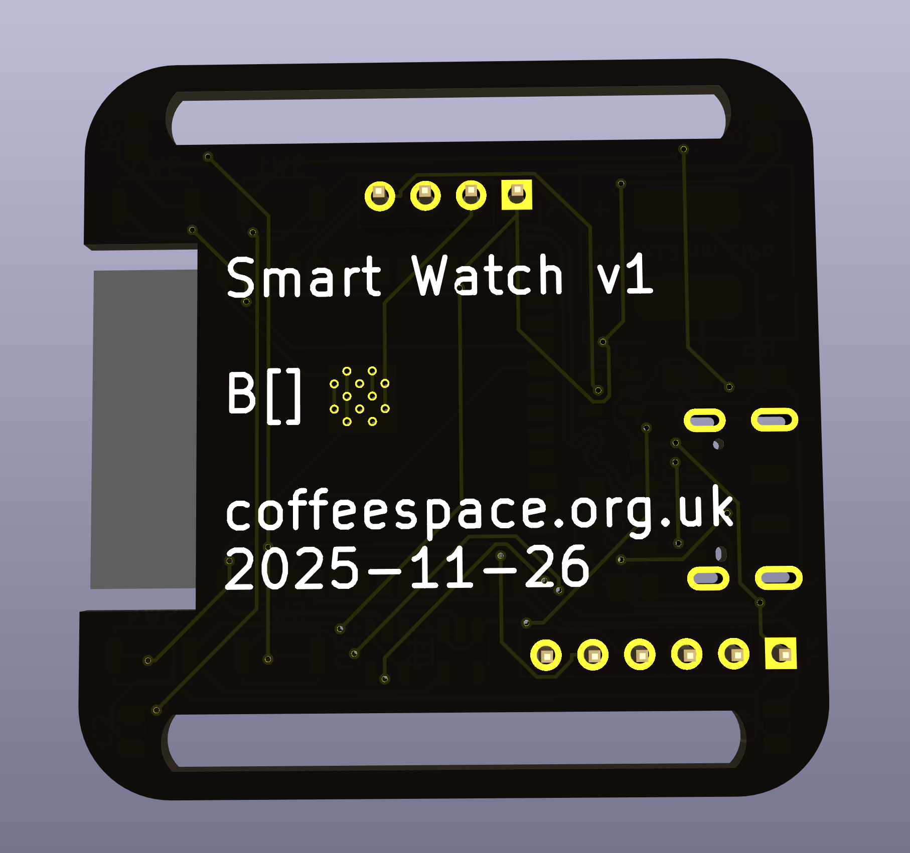
As you can see in the 3D render, there are clear cut-outs for a watch strap. I look to further reinforce this with the 3D printed chassis. The chassis is expected to attach as a “press fit” to secure it in place.
Soldering will need to start with the surface mount components, then the through-hole components, then finally the LiPo. The LiPo will be a pain, but time will need to be taken to ensure it is not directly touched by heat.

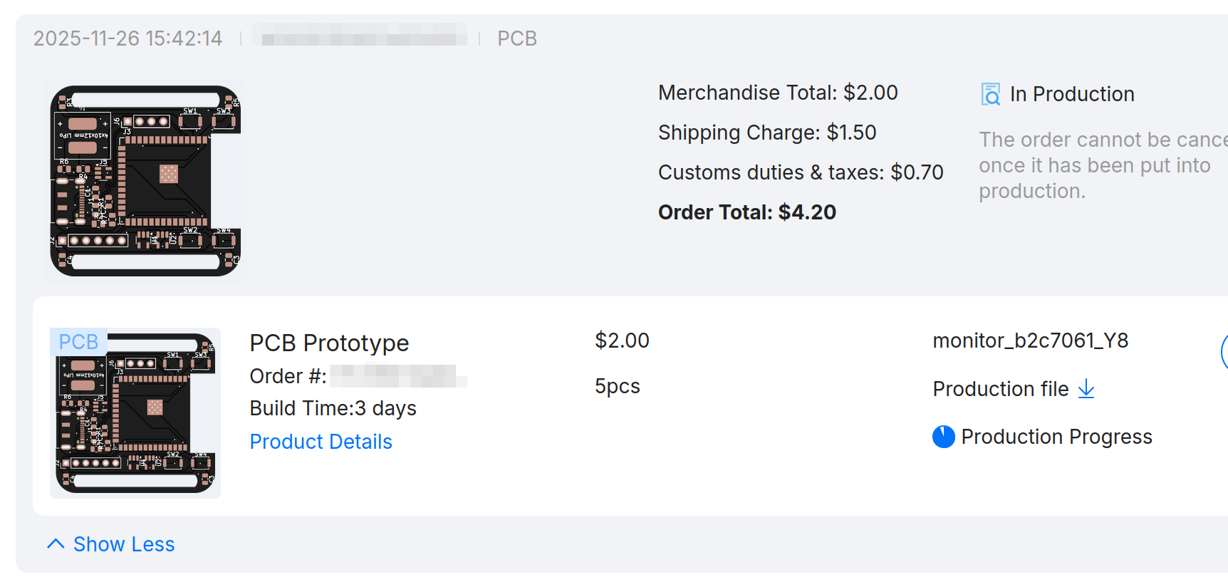
The PCB is sent for manufacturing, and I got quite a good deal on it. Five PCBs for $2, $1.50 shipping charge from China, $0.70 tax, for a total of $4.20. It’ll take a little while to arrive, but everything does.
The real downside is that I didn’t get a stencil. I’m thinking that I could probably cut one out on the vinyl cutter, or make a cardboard single-use stencil.

I was surfing the World Wide Web as I sometimes do, and I came across an LLM netlist checking tool. I plugged in the datasheets for the ICs I use, and gave the following prompt:
“It is a small ESP32 based smart watch with two input buttons, and an OLED display via I2C. There is a battery charge circuit for a single cell LiPo, a voltage I2C ADC to monitor battery voltage, and a 3V3 voltage regulator for the ICs.”
I wasn’t expecting much, I had already sent the board off to be manufactured. But after a few minutes, it generated this:
Overview
Key blockers before layout: the Li-ion charger is effectively unpowered, the 3.3 V rail lacks both the correct regulator variant and the minimum capacitors, and the battery monitor will overdrive its ADC input. Details by subsystem follow.
1. Power-input & Li-ion charging (U2 MCP73812, J1 USB-C, J4 battery)
- Charger supply/enable not wired: Pins VIN (pin 4) and CE (pin 1) of the MCP73812 share net N$11, but N$11 never reaches the USB 5 V rail, so the IC never powers up and CE never sees the required logic high. Tie both pins to the 5 V source and keep CE accessible if you plan to gate charging.[^mcp-pin]
- Mandatory capacitors missing: The charger needs ≥1 µF from VDD to GND and ≥1 µF from VBAT to GND for stability.[^mcp-cap] Add them close to the IC.
- Charge current check: R7 = 2 kΩ programs ≈500 mA fast-charge current.[^mcp-rprog] Confirm the USB source, battery, and PCB traces can safely handle that.
- Battery connector: Nothing obviously wrong; just ensure pack protection/NTC (external) is addressed elsewhere.
2. 3.3 V regulation (U1 TLV7xx, 3v3 net)
- MPN/value mismatch: Net 3v3 relies on U1, but the value is TLV70012 (1.2 V output). Verify the intended part; if you need 3.3 V pick TLV70033/TLV74033 etc.
- Input/output caps missing: TLV74x devices require at least one 1 µF ceramic on VIN and one on VOUT located close to the pins for stability and transient response.[^tlv-cap] Add them.
- VIN source: Once U2 is fixed, route USB 5 V (or battery when USB absent) cleanly into VIN with appropriate filtering.
3. MCU & digital core (J3 ESP32-S3-WROOM-1, SW1–SW4, R3–R6, C3–C4)
- Decoupling absent: The module needs the recommended 22 µF bulk plus 0.1 µF high-frequency capacitor right at its 3.3 V pins.[^esp-supply] Add them on the 3v3 net.
- Boot/strap networks: RC networks (R3/C3, R5/C4) and buttons appear to target strapping pins. Double-check the chosen resistor values meet Espressif’s strap logic levels and that any buttons pulling to 3.3 V have corresponding pulldowns or rely on internal ones.
4. USB interface (J1, C1–C2, R1–R2)
- VBUS usage: Currently 5 V is only on J1; extend it to the charger and any other circuits needing it. Consider adding input reverse-polarity or surge protection if needed.
- Signal conditioning: 47 pF shunts on D± may be aggressive; ensure they meet USB FS requirements once you know trace lengths. No glaring mistakes otherwise; CC resistors (R1/R2) look correct.
5. Battery monitor / I²C bus (J5 “MCP3021”, R7, J6 connector)
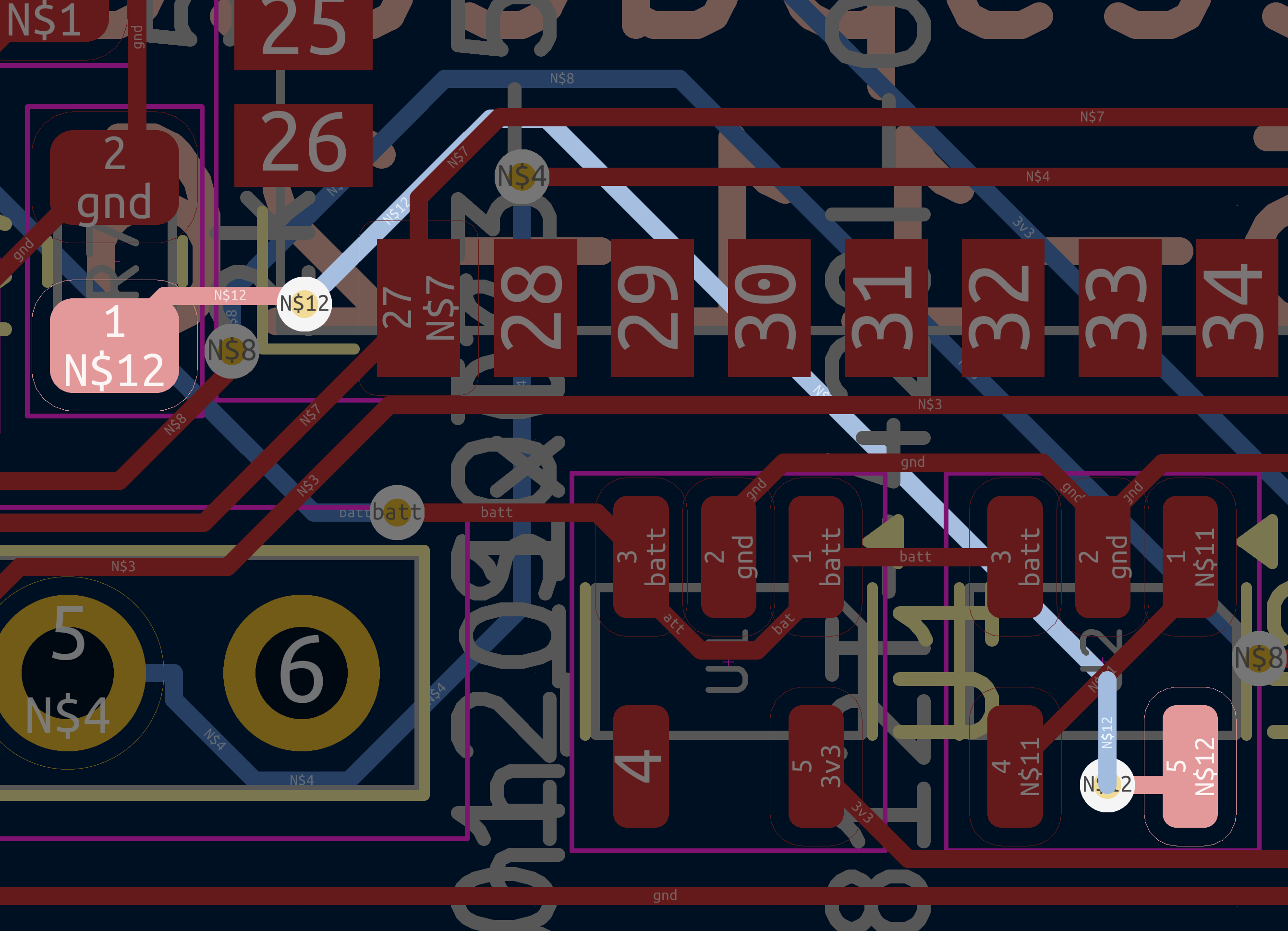
- Analog input over-voltage: MCP3021’s AIN must sit between VSS and VDD.[^mcp-ain] Here AIN (pin 2) is tied to batt while VDD (pin 4) is 3.3 V, so AIN can reach 4.2 V and violate the spec. Fix by adding a resistor divider (and optional RC) or powering the ADC from the battery and level-shifting I²C.
- Add I²C pull-ups: Nets N$13/N$14 lack pull-up resistors. Provide ~4.7 kΩ to 3.3 V so both the MCP3021 and the OLED connector (J6) have a defined bus idle level.
- Bus voltage domains: If you decide to run MCP3021 at battery voltage, include appropriate level shifting to protect the ESP32 pins (absolute max VIO ≈ VDD + 0.3 V).[^esp-io]
6. User inputs & connectors (SW3/SW4, J2, J6)
- Buttons simply short pins to 3.3 V; ensure firmware enables the needed pulldowns (or add resistors) to avoid floating inputs. Otherwise no electrical issues spotted.
- Programming header (J2) and OLED connector (J6) look consistent with shared I²C/SW nets.
Next steps
- Rewire U2 VIN/CE to USB 5 V, add the required 1 µF caps on VIN and VBAT, and confirm your intended charge current.
- Substitute the correct 3.3 V LDO variant and place the mandatory input/output capacitors; add the ESP32 bulk/decoupling caps.
- Protect the MCP3021 input (divider) and add I²C pull-ups; reassess level compatibility if the ADC runs from the battery.
- After these fixes, rerun ERC/DRC before moving to layout.
Addressing the points made:
And what’s worse, is that it should be!
0009 # monitor.py
0010 power = {
0011   "batt": v_batt,
0012   "5v": v_5v,
0013   "3v3": v_3v3,
0014   "0v": v_gnd,
0015 }
0016 # ...
0017 man = MCP73812T_420I_OT(power)
0018
0019 # mcp73812t_420i_ot.py
0020 if "5V" in power :
0021   self.man[4] += power["5V"]
Can you spot it? It’s defined as 5v in the power net and
5V in the check! It fails silently! Making it raise an
exception if the label is not found immediately shows the issue:
0022 # mcp73812t_420i_ot.py (revised)
0023 if not "5V" in power :
0024   raise Exception("No 5v found!")
0025 self.man[4] += power["5V"]
0026   File "/env/src/shared/mcp73812t_420i_ot.py", line 33, in __init__
0027     raise Exception("No 5v found!")
0028 Exception: No 5v found!
Note: The first version will need to somehow get 5V from the USB bus, otherwise it will not be able to charge the LiPo. There is no way to easily achieve this, so I will need to have a think about it.
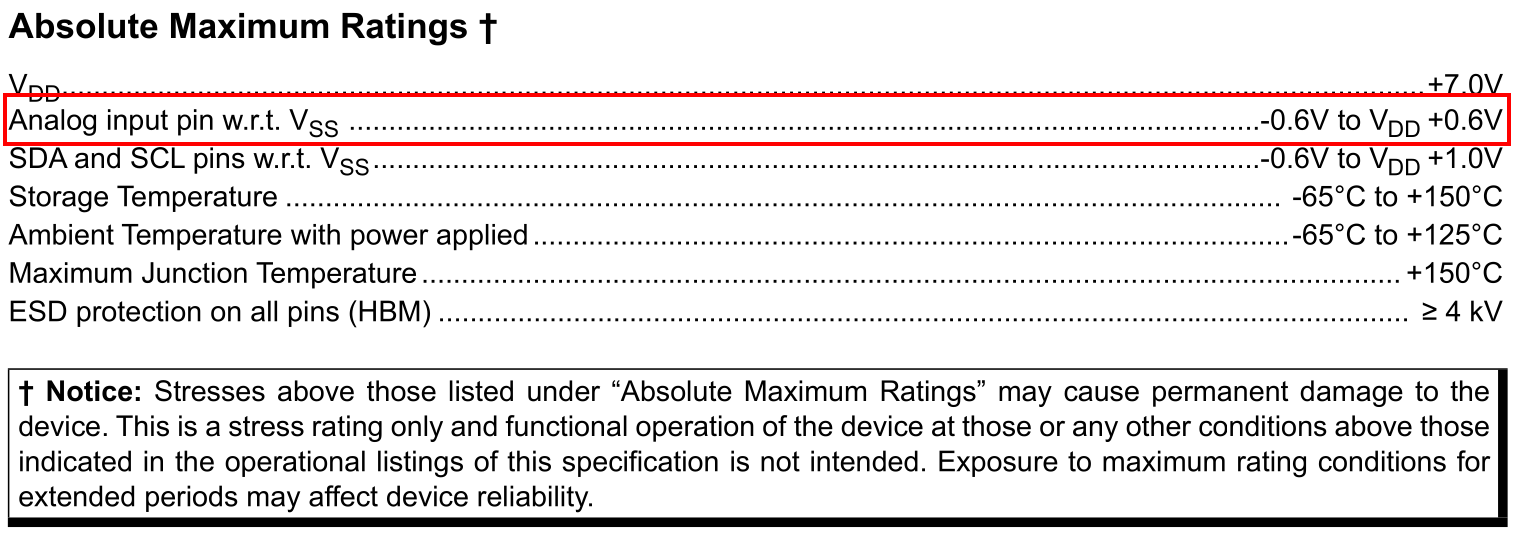
The absolute limit is VDD + 0.6V, so 3.3V from the regulator, bringing us up to 3.9V. 3.9V to 4.2V is not too crazy, maybe we could get away with it?
This all said, I wanted to check if there are any known side effects of missing the input/output capacitors:
“What can be the consequence of missing the 3.3V input/output capacitors? It is believed that the ESP32-S3-WROOM-1 module has it’s own internal capacitors, and that the capacitance of the board is sufficient?”
Leaving out the regulator’s 3.3 V input/output capacitors is risky:
- Regulator stability: The TLV740 family explicitly requires at least 1 µF of ceramic capacitance on both VIN and VOUT for loop stability and transient response (§7.1.2, TI TLV740 datasheet SBVS401B). Without them the LDO can oscillate, overshoot, or momentarily drop out, which will show up as random brown-outs or crashes of the ESP32, OLED, and ADC.
- Transient/PSRR degradation: Even if the circuit seems to work on the bench, load steps from the ESP32’s radios or display can inject noise back into the rail. Missing capacitors greatly reduce PSRR and worsen line/load transients, so RF performance, ADC readings, and I²C integrity suffer.
- Module expectations: The ESP32-S3-WROOM-1 reference design still places bulk (≈22 µF) and high-frequency (0.1 µF) capacitors right at the 3V3 pin (Fig. 7, esp32-s3-wroom-1 datasheet v1.4). The module’s internal bypassing only covers on-module circuitry; it assumes the host board supplies its own local decoupling.
In short, rely on the datasheet values—place the required ≥1 µF ceramics at the regulator pins (plus the usual 10 µF/0.1 µF pair near the module). Skipping them invites instability and erratic behavior.
Okay, okay, I will put some capacitors in the new design.
And lastly, what the consequences are for running the ADC out of spec:
“MCP3021 analogue input can be VDD + 0.6V, where VDD should be 3.3V and the maximum will be 3.3V + 0.6V = 3.9V. The battery fully charged is 4.2V. What will happen to the IC?”
According to the MCP3021 datasheet, the analog input pin (AIN) must always stay within VSS –0.3 V to VDD + 0.3 V (see “DC Electrical Specifications,” DS20001805C, p. 3). With the device powered at 3.3 V, any voltage above about 3.6 V violates that limit. Driving AIN with the full 4.2 V from a freshly charged Li‑ion cell forward-biases the input’s internal ESD/clamp structures. In practice that:
- Forces current through the protection diodes into the 3.3 V rail, which can pull VDD above its nominal value, upsetting the ESP32 and other loads.
- Produces gross conversion errors because the sampling capacitor is no longer referenced correctly.
- Risks long-term damage: repeated or sustained over-voltage can overheat the clamp diodes or core circuitry, eventually destroying the ADC.
You should scale or buffer the battery voltage so AIN always remains within the allowed range—e.g., a resistor divider sized to keep the maximum input ≤3.3 V (or add a buffer/level shifter if you need very high input impedance), and optionally include a small series resistor to limit any fault current.
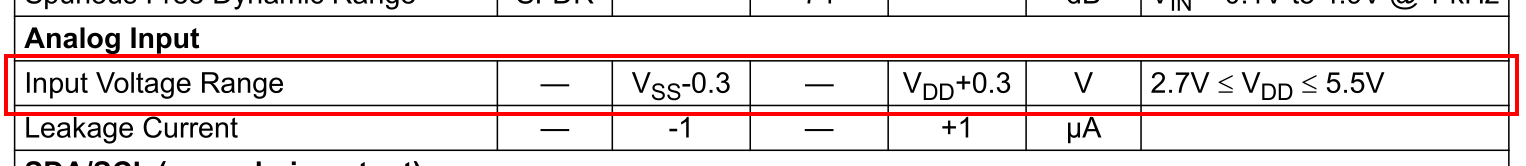
Well, the usable range is actually limited to within VDD + 0.3V… Maybe it could still be used to detect low battery voltage?
Ah, and herein is the problem - those damn diodes. If we drive the analogue input too high, then it will try to drive VDD. Damn.
Note: The ADC cannot be populated in the first design.
Hmm, I think I will be looking for a new ADC in the next design, or I need to be really clever about reliably measuring the 4.2V. To measure 4.2V with this current IC I would need to drive VDD with at least a steady 3.9V, damn.
Is using an LLM for netlist inspection worth it? It seems so! I have no idea how many hours this may have saved me in debugging time!
Hopefully all of the parts arrive soon enough and the first revision can be made.
It looks as if micropython make using the OLED display quite easy
with the ssd1306
library, offering a framebuffer and some handy drawing functions.
I may consider bringing back the pt-draw library to draw lightweight vector graphics. Maybe I could try parsing some sub-set of the SVG library via the micropython XML library xmltok (or perhaps uxml2dict to get a dictionary) and just support line segments (makes designing in external editors easier).
I still need to figure out how to communicate with the ADC to read the battery level, but this should be quite simple via I2C. It’s important that it can be read, though, as it will be a large part of the power saving strategy.
The next step will be to build out the firmware development and deployment system to make my life easier.
At the time of writing this part, everything is already sent off!
In a future revision, there is a viable path to bring the cost down. After a chat with the people at the local hackspace, the best approach is likely a resistor ladder, but via a MOSFET. That circuit looks like so:
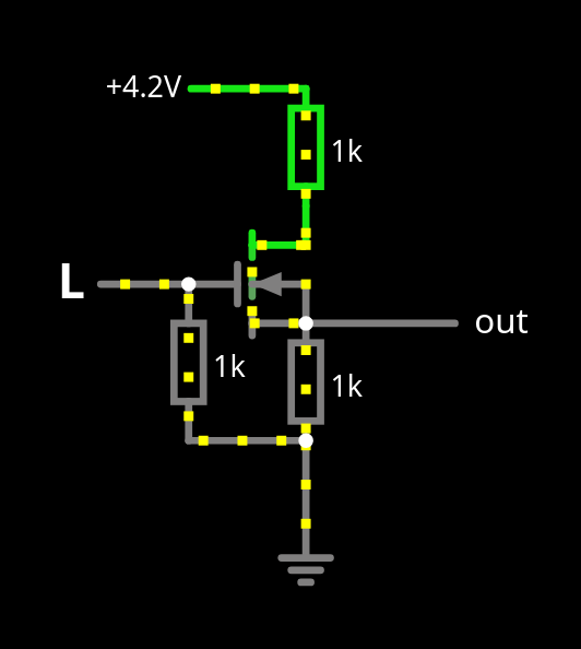
This is with the DMN62D0U-7, an 8p IC. I calculated the MOSFET Beta to be at 0.8 (, , Threshold ). In the simulation (with resistors all set to 10k) the off-current is ~200nA and the on-current is ~700uA, which seems quite acceptable.