
The idea of this project is to build a very simple games console that can be programmed with various very simple games. I’m thinking space invaders, tetris - games along these lines. It’s not going to be the most powerful device in the world by any means, but it should be fun! I also enjoy seeing what can be done with as little resources as possible and this is going to be something that tests those limits.
The motivation behind this project is the many projects on Hackaday seen every day and thinking “I could do that!”. The Game Boy in this authors opinion was an awesome console and many fond memories from childhood were spent playing that game.
This I guess is a tribute to those memories and the awesome engineering that went into them. I’m not quite sure my shoddy engineering is a good tribute to these blasts from the past but ho-hum.
The following is the list of requirements I have for the device:
NOTE: Pictures will come at a later date.
The following is the plan I came up with to make sure the idea is feasible:

As you can see, it will sure be a close call! We have zero spare pins if there are any problems, so the risk is fairly high. The backup plan is to use an Arduino Nano as there are many more pins, although this means the loss of the form factor.
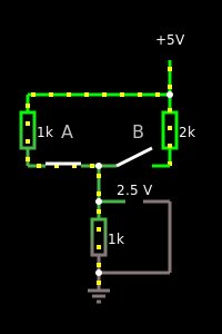
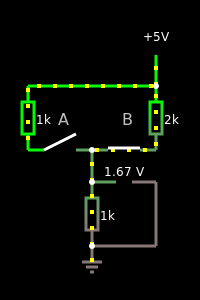
I used the Falstad circuit emulator to check that my logic was correct - which it wasn’t, hence the resistor value change in the following images:
Logic: A !B
Logic: !A B
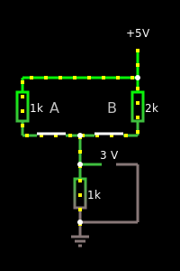
Logic: A B
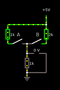
Logic: !A !B
Of course, the input voltage will be 4.2V and could drop down to 3.7V as the battery depletes. The following is a table generated from the circuit emulator:
0001 Voltage  A  B  Measurement (V)
0002 4.2      0  0  0.0
0003 4.2      0  1  1.4
0004 4.2      1  0  2.1
0005 4.2      1  1  2.5
0006 3.7      0  0  0.0
0007 3.7      0  1  1.2
0008 3.7      1  0  1.9
0009 3.7      1  1  2.2
As you can see, there’s no overlap as the voltages go down meaning that we can check for a voltage range to see what combinations of buttons has been pressed. As the voltage drops down below 3.7V, we should certainly stop using the battery to prevent damage, hence bad button presses isn’t an issue.
Following this successful simulation, we have the following diagram for all of the buttons which also attempts to act as the PCB layout:
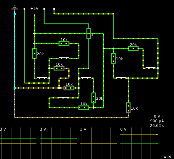
Button layout for all six buttons in a game configuration (Source: Falstad file)
As can be seen from the circuit, using 10k and 20k resistors the entire circuit would have a 900uA current draw at worse. The ground and supply rails are also well isolated from one another, meaning that shorts should be better avoided. The components are also reasonably well placed away from one another, meaning that they should be solderable and the buttons pressable.
Drawn now is the schematic and the project files that built that using KiCAD here. There is likely little need for PCB layout as the board will be custom created using some copper plated fibre glass and etching solution.